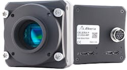
Chromasens has launched a machine vision system that detects defects on silicon wafers invisible to the naked eye, such as sub-pixel sized scratches, cracks, and stains. The wafer inspection system comprises a Chromasens allPIXA evo 15 k CxP4 mono camera, Myutron XLS05 lenses, an XCL4 LED controller, and Corona II lighting with coaxial light modules for dark field and bright field illumination. The allPIXA evo 15 k CxP4 mono camera is equipped with a trilinear CMOS line scan sensor. Compatible with the CoaXPress (CXP) interface, the camera achieves full resolution of 15 k at line rates up to 68.4 kHz. The allPIXA evo 15 k CxP4 camera included with the system can trigger up to four different flash controller channels synchronized to its line acquisition using a multi-channel LED flash. By integrating both Corona II bright field and dark field illumination, the system acquires multiple lighting conditions in one scan of the wafer. Users can choose from a variety of options, including the number of cameras, color or mono imaging, field of view (FOV), and the illumination setup.
To Learn More:
Contact: Chromasens
Headquarters: Konstanz, Germany
Product: wafer inspection system
Key Features: Compatible with the CoaXPress interface, Full resolution of 15 k at line rates up to 68.4 kHz, trilinear CMOS line scan sensor
What Chromasens says:
View more information on the wafer inspection system.
Share your vision-related news by contacting Chris Mc Loone, Editor in Chief, Vision Systems Design.